
Electron Beam Microscopy: Spellman's Role and Applications
by Marcus Foxwell
Spellman's electron beam microscopy solutions provide the necessary voltages for imaging while maintaining extreme accuracy and precision.
 Electron microscopes are used across a range of industries and have everyday applications, while playing a role in all our lives. Fields such as materials science, medicine, and forensics have all been revolutionized by advancements in the use of these microscopes.
In cancer research, for example, electron beam microscopy (EBM) helps doctors spot abnormal cell structures early, improving detection and treatment. In materials science, scientists can explore and understand nanostructures, driving innovations in electronics and energy-efficient technologies. In forensics, a detailed analysis of residues and fibers plays a crucial role in solving crimes.
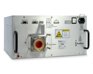
Spellman is the world’s leading supplier of precision high voltage solutions for electron microscopy. Our EBM solutions provide the necessary voltages to achieve the imaging using an electron beam while maintaining extreme accuracy and precision. Units range from 5 kV up to 120 kV depending on the customer's application. Most of Spellman’s products consists of bespoke solutions for customers; however, a standard range is offered.
Powerful Techniques for Highly Detailed Imaging
 Scanning electron microscopes (SEM) are widely acclaimed for their remarkable precision in providing highly detailed, three-dimensional images. They use a high-voltage beam of electrons to interact with the surface of a sample and detect emitted and backscattered electrons, resulting in a high-resolution image. The main components of SEM include electron beam generation, beam focusing, sample interaction, image detection, and formation.
Electron beam generation is achieved using an electron gun such as a Spellman EBM power supply unit (PSU). The electrons are accelerated toward the specimen using typical voltages between 5 kV and 30 kV. This is called acceleration voltage, the main high voltage output on Spellman's EBM PSU. Voltages in a SEM can reach up to 75 kV to increase the resolution and penetration depth into the sample. The typical magnification range of this microscope is 20 times to 1 million times. For reference, a normal light microscope has a magnification of 2,000 times.
The process of focusing the beam is of utmost importance in achieving high-resolution image generation. A beam is meticulously focused using a series of electromagnetic lenses. The beam then scans across the sample, with some electrons and radiation being absorbed, deflected, or emitted. Detectors capture these emitted electrons, known as secondary and backscattered electrons. A computer then uses the captured electrons to generate an image of the specimen.
Transmission electron microscopes (TEM), on the other hand, focus on imaging the internal structure of materials at near-atomic resolution, unlike SEMs, which provide three-dimensional images. TEM produces two-dimensional images by passing an electron beam through the sample, which is then captured by a CMOS (complementary metal-oxide-semiconductor) camera. Unlike SEM, which detects deflected electrons, TEM captures those that pass through the sample, offering detailed insights into internal composition and morphology. These systems require voltages in the hundreds of kilovolt range while maintaining an extremely high level of accuracy. The typical magnification range of this type of microscope is 50 times to 50 million times.